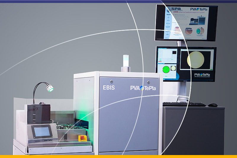
Our base systems allow a flexible integration of various inspection capabilities

Optical inspection

Our base systems are designed to allow a flexible integration of various inspection capabilities. The possibilities range from manually operated inspection workflows up to full automation with image analysis with specific algorithmic inspection tasks. For this purpose we provide compact handling solutions for loading wafers or frames onto various inspection systems.

Contact us

How can we help you?
Let´s talk!

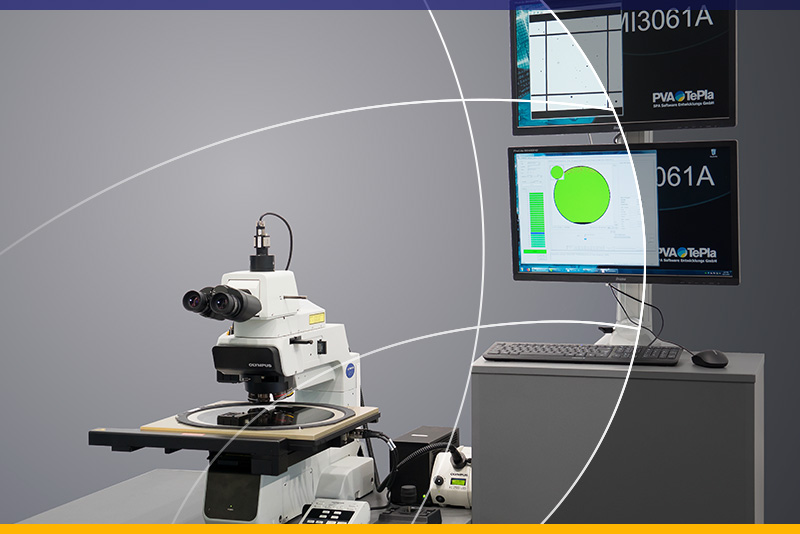
Microscope Inspection (MIx models) / wafer/frames up to 12”

Manual wafer or frame loading

Purpose of Microscope Inspection

Automatic or manual visual microscope for wafer inspection up to 12” diameter, loaded manually by hand onto a motorized xy table.

Key benefits:

  • Micro defect inspection (>0.6µm)
  • Pragmatic hardware concept consisting of microscope, camera and xy motorized table
  • Manual loading of framed wafers by hand
  • Simple frame chuck holder with mechanical or vacuum frame fixation
  • Compatible for 4” 5” 6" 8" and/or 12" wafers on frame

MIx Options:

  • Metrology software addon
  • 3D surface measurement technology
  • Infrared (IR) inspection technology

UL200 wafer loader

Automatic wafer or frame loading

Purpose of UL200 wafer loader

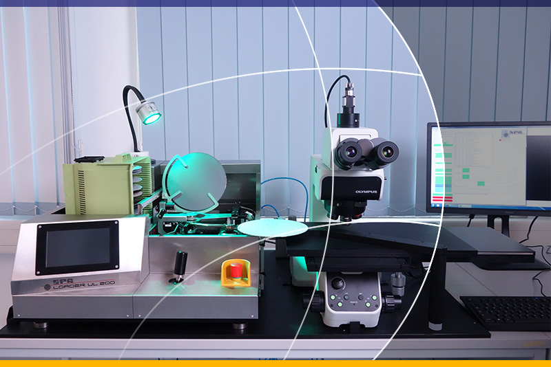
The UL200 serves as a compact and fast tabletop wafer loading system for up to 8” bare wafers with customer-specific requirements.

Key benefits:

  • Wafertype-specific and dynamic wafer detection for safe loading from cassette
  • Automatic loading of 100-150mm or 150-200mm wafers
  • Prealignment of wafer position and rotation
  • Single and multi wafer handling to xy table
  • Docking compatibility for manual or automatic xy tables
  • ID Reading integrated within UL200
  • Footprint approx. [mm] 620x630
     

UL200 Options:

  • Illuminated top/back macro defect inspection
  • Flat/notch alignment sensors for transparent wafers
  • TAIKO and thin wafer handling
  • SMIF wafer loading in UL200-SMIF version
  • Framed wafer loading in UL200F version
  • Remote interface for external control (e.g. via VCP)
  • SECS/GEM compatible interface

Universal Loader Microscopes (UL20x models) / wafer/frames 8“

Automatic wafer or frame loading

Purpose of Universal Loader Microscopes

Automatic or manual visual microscope inspection of up to 200mm wafer, loaded automatically by the UL200 wafer loader from cassettes onto a motorized or manual xy table.

Key benefits:

  • Compact tabletop wafer loading system
  • Automatic loading of 100-200mm wafers with a compact waferloader
  • Microscope with remote interface control and laser autofocus
  • Micro defect inspection (>0.6µm)
  • Footprint approx. [mm] 1650x630
     

ULx options:

  • Metrology software addon
  • 8” framed wafer cassette compatibility
  • SMIF wafer cassette compatibility
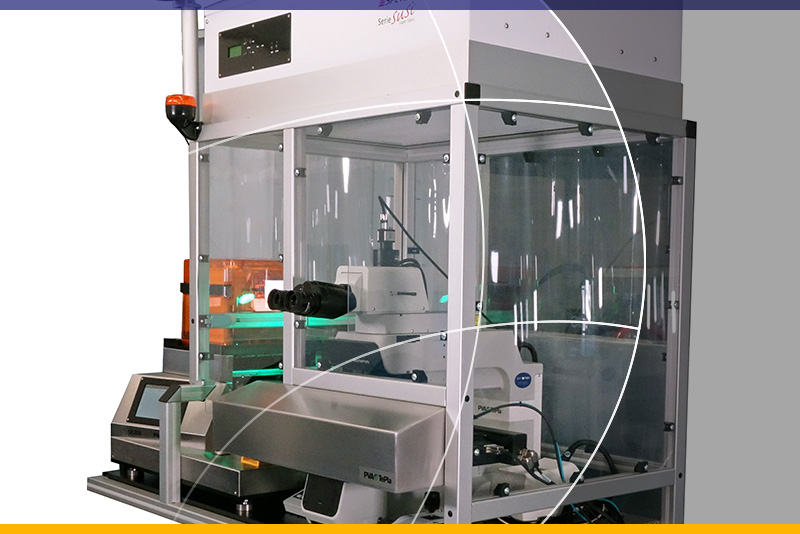
  • Enclosure with clean air flowbox
  • Infrared (IR) inspection technology
  • SECS/GEM compatible interface

BridgeTools (BTx) / wafer/frames up to 12“

Automatic wafer or frame loading

Purpose

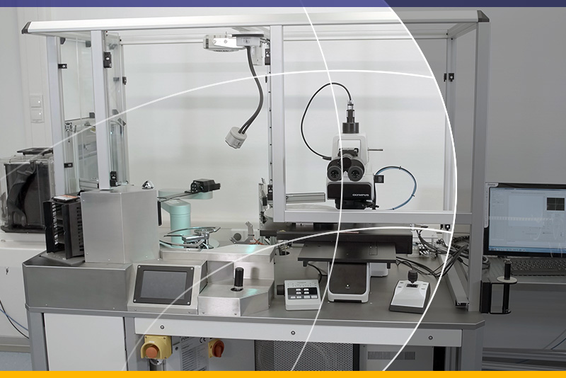
Automatic or manual visual microscope for wafer inspection up to 12”, loaded automatically by a robotic handler from open or FOUP cassettes onto a motorized xy table.

Key benefits:

  • Automatic loading of 200-300mm wafers and frames with a robotic wafer handler
  • Microscope with remote interface control and laser autofocus
  • Micro defect inspection (>0.6µm)
  • Footprint approx. [mm] 2400x1100
     

BTx options:

  • Metrology software addon
  • Framed wafer automatic loading
  • Infrared (IR) inspection technology
  • Edge wafer handling
  • SECS/GEM compatible interface (supports GEM200, GEM300)

Enhanced Backside Inspection System (EBIS) / wafer up to 8“

Automatic wafer or frame loading

Purpose

EBIS synchronizes visual defects located on a wafer backside to the frontside chip structure. Optimize your yield by precise automatic detection or manual marking of only the affected fail chips, and thus avoiding oversized fail area classifications!

“We make your wafers transparent”

Key benefits:

  • Fast automatic loading and scanning process (up to 250 WPH)
  • Full automatic macroscopic defect detection on wafer backside (defects >60µm)
  • Optional visualization of complete wafer backside on the screen for defect marking or reviewing AOI results
  • Transparent wafer frontside overlay on backside image during review process
  • Automatic wafermap edit when backside defect is detected based on given threshold parameters

Ebis options:

Also available as standalone system or integrated in third party equipment environment.

Immediate Contact

slideoutcontact
Please complete all fields marked with *.
Please solve the following question:
captcha

PVA SPA Software Entwicklungs GmbH
Seifartshofstraße 12-14
96450 Coburg, Germany

Phone: +49 (0) 9561 7947-0

Request Product Information

Produktinformation EN
Please complete all fields and choose the product you would like to learn more about. The product data sheet will then be e-mailed to you. Please understand that in order to preserve our natural resources, we do not send out any printed material.
Please complete all fields marked with *.
Please solve the following question:
captcha

I am aware that when I make contact using this contact form, my data will be stored to facilitate the further processing of my inquiry and subsequent inquiries.