-
The product portfolio of PVA SPA Software Entwicklungs GmbH implies fully automatic systems for quality control of semiconductor frontend and backend products. By the usage and ongoing development of image analysis modules we offer automatic optical inspections of wafers on 2D images and also high precision 3D surface profiles. Our customer-focused approach allows us to provide the exact solution customers are looking for.
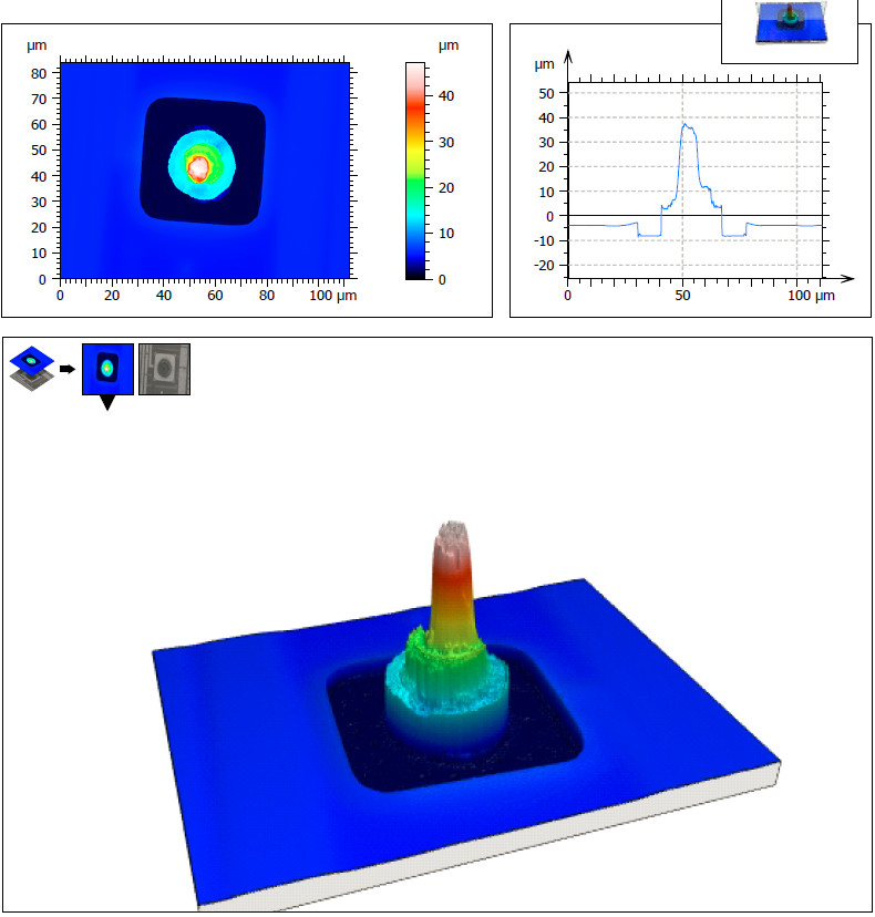
Bump & Ball inspection AOI package
- automatic 3D profiling of bumps and balls
- threshold definition for top, medium and lower bump/ball surface measurement
- adjustable magnification (if lens changer exists)
- Inspection result output in wafermap or in CSV result file
- Usage of sample inspection algorithms possible
- Third dimension resolution: 5 - 50nm (depending on material)
- Lateral resolution: 0,5 – 8µm/px (depending on used objective lens)
Chip Reference Model AOI package
- Chip-to-chip comparison (fixed RM training per wafer type), support for different zones with different weights
- Chip-to-chip comparison without type-dependent image processing script (dynamic RM training per wafer)
- Support for sample measurement (configurable percentage)
- Programming robust RM inspection scripts for 5 different types of wafers
- Integrated VSE (Visual Script Editor) for analysis and script programming
Inkdot inspection script AOI package
- 100% inkdot quality assurance
- Ink splash detection on good dies
- Automatic reinking of inkdot failures
- Inkdot size (min/max) control
- Inkdot position control
- Inkdot shape control (roundness, aspect ratio)
- Ink on pass chip detection
- Individual inspection parameters for edge dies
Probemark inspection AOI package
- 2D distance control of scrub to pad edges
- Surface area control of scrub within pad (in %)
- Optional 3D profiling of scrub depth and height
- Usage of sample inspection algorithms possible
- Third dimension resolution: 5 - 50nm (depending on material)
Lateral resolution: 0,5 – 8µm/px (depending on used objective lens)
Sawing inspection AOI package
- Die-to-die distance measurement on top sawing edge
- Die-to-die distance measurement on bottom sawing edge
- Sawing edge to chip sealring distance measurement
- Chip size measurement on top sawing edge
- Chip size measurement on bottom sawing edge
- Chip tilt comparison to xy alignment
- Sawing street profile in 3D with interface to MountainsMap application
- Third dimension resolution: 5 - 50nm (depending on material)
- Lateral resolution: 0,5 – 8µm/px (depending on used objective lens)
-
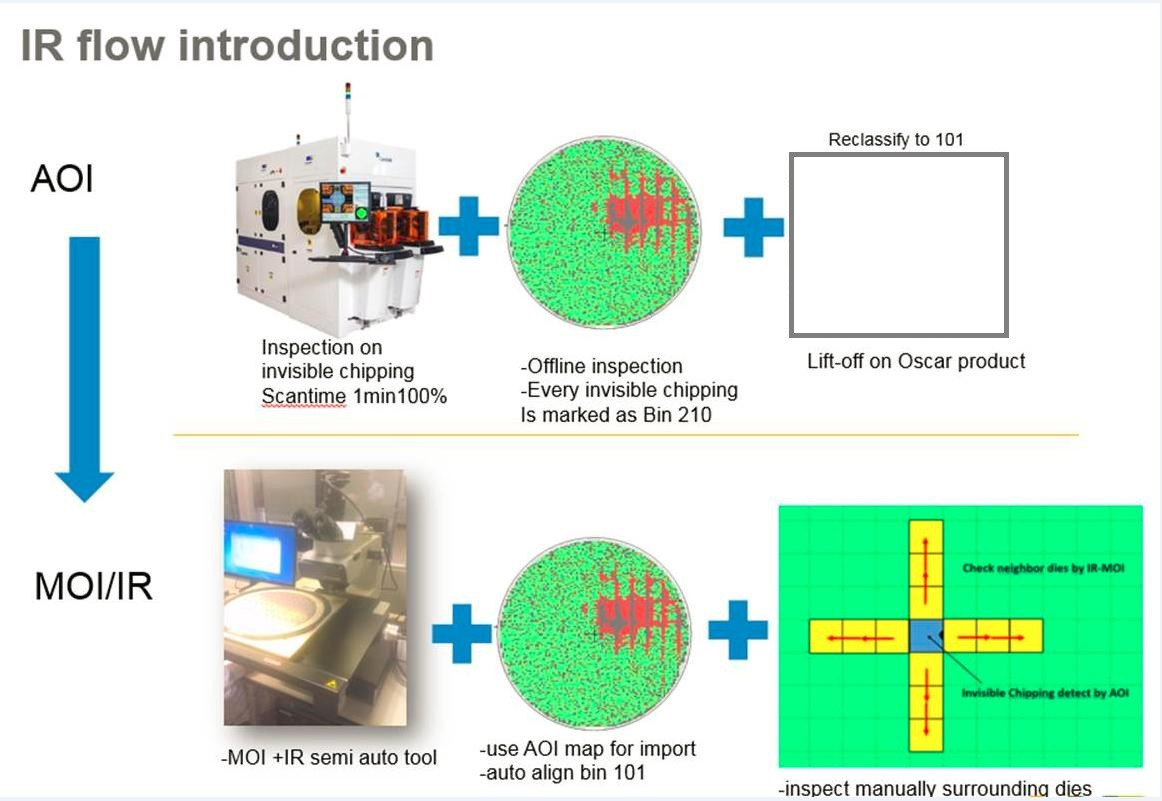
The product portfolio of PVA SPA Software Entwicklungs GmbH implies manually operated systems for quality control of semiconductor frontend and backend products. By the usage and ongoing development of our software modules we offer semi-automatic workflow sequences for increasing the operator inspection efficiency. Our customer-focused approach allows us to provide the exact solution customers are looking for.
KLARF import / review / export module
- KLA result file (KLARF) import
- KLA result file (KLARF) defect review
- Supporting KLARF Version 1.2
- Supporting several defects per chip
- Table/list of defects within a chip
- Stage movement onto selected defects
- Support of error classes
- Reclassify error classes
- TIFF conversion for defect images
- Process support for image acquisition (manual, semi-automatic, automatic)
- Automatic deleting of KLARF and image data after n days on computer
- Automatic calculation of the magnification for defect image acquisition
- KLA result file (KLARF) export without data loss
Sample inspection algorithm package
- Preconditions: Wafermap import converter and motorized xy table
- Chip prepositioning
- Defined list of positions per chip and wafer
- Chip-coordinate-fine inspection algorithm (Sample, AQL, LTPD, edge, 100%)
- Move to Chip thru mouse-click in the mapdisplay with adjustable relative offset in chip


