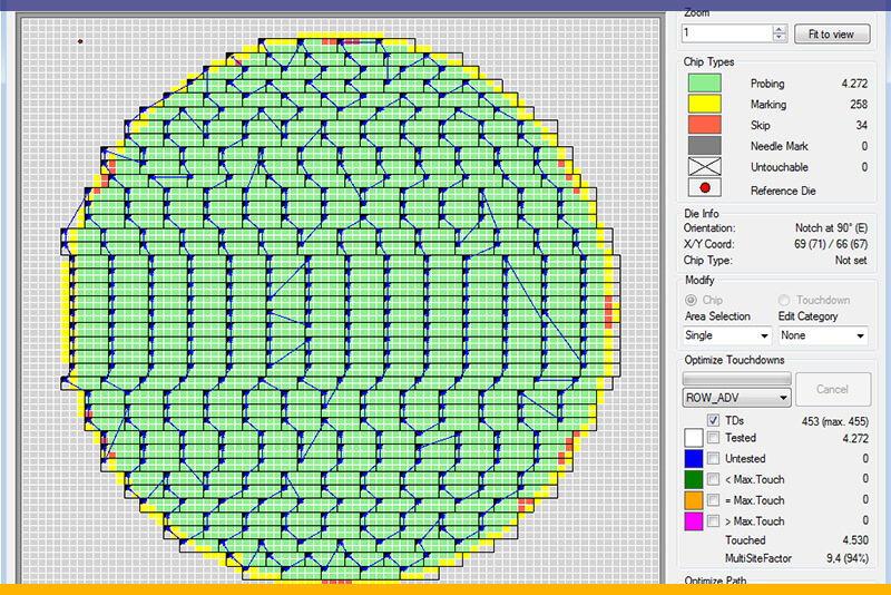
The MSO Stepping Optimizer is a standalone application for optimizing the multi-site probing process in your electrical wafer test area.
Highlights:
- Reduce touchdowns and minimize probing time
- Increase efficiency of your prober equipment with only one MSO user license
- Optimize your probing path (heat/speed improvement)
- Flexible Multi Site Layout Types: Solid, H-Columns, V-Columns, Chess, Skip, Solid free form, Rhombus, Diagonal, Multi Diagonal
Options:
- Find ideal probecard layout with the Automatic Layout Finder (ALF)
- Optimize the lifetime of your probecards with automatic site balancing (BAL)
- Full wafer probecard (FWC) layout creation
MSO optimizes multi-site probe card xy positions on wafer probers and allows the calculation of different stepping path sequences.
Key benefits:
- Calculation of minimum touchdown amount for testing an entire wafer
- Situation-dependent stepping path algorithms (shortest distance, x-meander, y-meander, hot probing, site balancing)
- Reduction of needle re-alignments by usage of hot probing stepping path algorithms
- One MSO standalone user license can generate optimized stepping data for your entire probe floor
The MSO can be upgraded with an Automatic Layout Finder (ALF) solution, which calculates the optimal probe card channel arrangement for a given wafer type.
Key benefits:
- Automatic calculation of the layout shape (channel arrangement) resulting the smallest amount of touchdowns required for testing a wafer product by consideration of the maximum amount of channels available for parallel testing
- Overview of all calculated layout shapes and their MSO result data in a table allowing interactive touchdown preview
- Consideration of constraints for limiting ALF results (max. probe card xy dimension, amount of skips in x or y between active probing channels)


