Environmental conditions for chip production
Microelectronic devices as part of electronics have become part of our daily lives - whether in smartphones, smart homes or smart cars with intelligent optical sensors and emitters, as well as corresponding logic and memory devices. Advanced devices of this kind require sophisticated manufacturing equipment and special care in handling, including during subsequent quality inspection. For this reason, semiconductor wafer production is highly automated. However, it is selectively supplemented by targeted manual inspection processes, with most operations being carried out in a cleanroom environment.
Higher quality requirements in LED manufacturing
The desire for ever higher yield and reliability of the end products is also the motivator of the continuous improvement process in LED manufacturing. Progressive miniaturization and increases in power density demand these improvements.
OSRAM Opto Semiconductors in Regensburg, part of the ams OSRAM group, is one of the market leaders for optical solutions. For this reason, the company is raising its quality standards in terms of air purity and protection against particle contamination at its visual post-control workstations. Microscope systems for post-inspection of sapphire, gallium arsenide (GaAs) or silicon wafers in LED manufacturing are usually open workstations in a clean room certified according to DIN EN ISO 14644-1.
To reduce particle generation by system operators, it is necessary to shield the wafers from external influences during microscopic inspection. Defined air purity should also be ensured within the inspection facility. For such an increased demand, the wafers are transported in closed cassettes with 25 pieces each between the different process steps. A machine must therefore have the ability to unlock such a cassette and also to lock it again at the end of the process. In the case of wafers with a diameter of 200mm, these are cassettes of the SMIF (Standard Mechanical Interface) type. In most cases, visual inspection of the optical quality of the surface condition of the wafers is carried out after lithographic and chemical processes. The system operators are responsible for the dimensional accuracy of the components and the absence of defects.
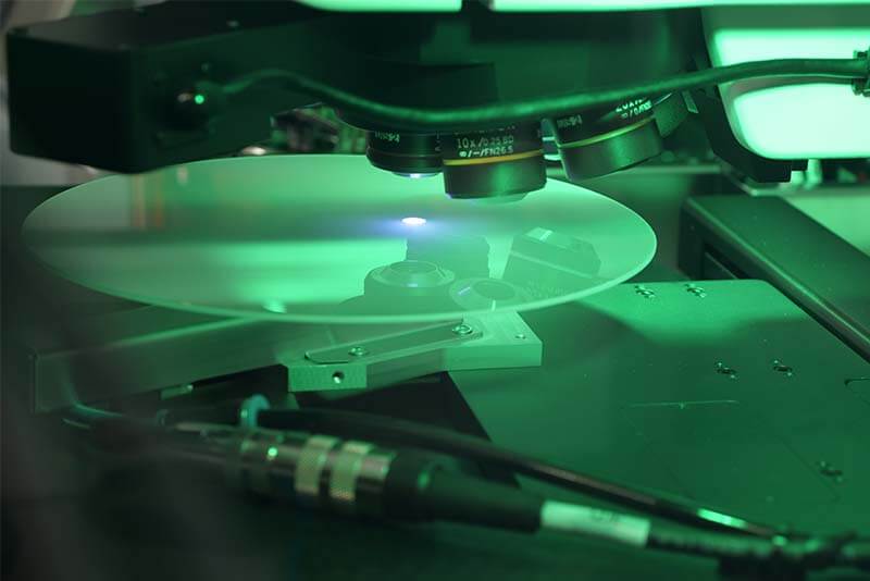
Figure 1: Sapphire wafer under MX microscope (Source: PVA SPA)
Partnership with system integrator from Bavaria
In the search for a suitable supplier of semi-automated microscope systems with an integration concept suitable for automated production, the choice fell on PVA TePla, in this case represented by its subsidiary PVA SPA Software Entwicklungs GmbH based in Coburg. Thanks to the already long-standing and successful cooperation, PVA SPA is a welcome supplier of optical microscopy for OSRAM OS. This is due in particular to the extremely high flexibility in the implementation of special process requirements. In addition to standardized system coupling using the SECS-GEM protocol, which is well-known in the semiconductor industry, this also includes the complete traceability of manual optical inspections through digital reporting to a higher-level production control system. PVA SPA can meet this trend with its microscope solutions and was therefore awarded the contract for new partially automated microscope solutions at Osram OS. The systems were also able to satisfy a corresponding profitability test by the customer.
Guided wafer inspection with KLARF (KLA result file) generation and simple operator control form a well embedded solution in the otherwise more automated manufacturing environment. The production and data control systems are thus automatically recorded after the semi-manual inspection and the line flow and booking lines are only slightly affected.
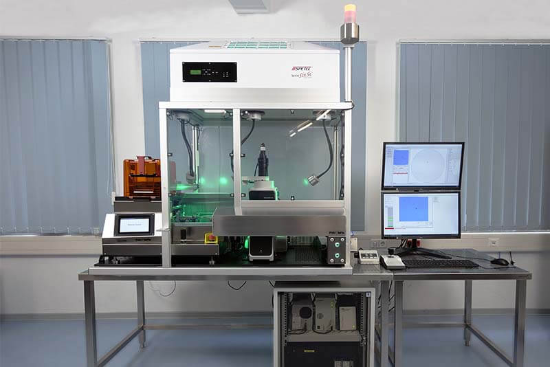
Intelligent Microscope Systems with SMIF and Flow Box
The newly designed microscope system includes a UL200 type wafer loader, but with the special feature of being able to open and lock SMIF wafer cassettes automatically. After unlocking, the wafers are loaded from the cassette into an encapsulated interior of the system. In this interior, a flow box located on the enclosure provides a downward laminar flow of pure air. The complete enclosure of the wafer loading, including the microscope, also protects the components from mechanical damage.
The MX semiconductor inspection microscope from Olympus Europe with modularly integrable laser autofocus and motorized XY stage can be completely controlled from the outside so that defined inspection tasks can be processed from the screen.
For the traceability of defects found on a wafer, these abnormalities can be measured in the image and added as digital information to KLARF, an industry standard for advanced wafer map functionalities. On the other hand, for the purpose of process improvement, such an intelligent microscope can also be used to target defects on the wafer that were previously found on other machines during automatic optical inspections (AOI).
Figure 2: Semiconductor microscope of the MX class, adapted to the inspection of wafers up to 300 mm (Source: OLYMPUS DEUTSCHLAND GMBH)
Figure 3: No microscopy without optics - the MX microscope is excellently suitable for UV fluorescence but also infrared inspection (Source: OLYMPUS DEUTSCHLAND GMBH)
![[Translate to EN:] MX Halbleiter-Inspektionsmikroskop von Olympus Europa mit modular integrierbaren Laserautofokus](/fileadmin/user_upload/SPA/pictures/olympus-online.jpg)
A high benefit for the user
It should be noted that the new microscopes completely fulfill their intended purpose. Particle measurements have shown that appropriate air purity inside the plant is essential. "With the SMIF microscopes, we have succeeded in providing our engineering and development colleagues in particular with a control system that enables analytical work in an automated process environment. Especially for basic developments and product improvements, a macroscopic and microscopic impression of the wafer material is indispensable. Whereas in the past we worked with images on drives, now the markings and images are linked directly in KLARF and can be viewed immediately and precisely positioned in the yield management system at the corresponding process stage," stated Dr. Robert Friedemann, Key Expert, Testing & Analytics, at OSRAM OS.
Despite state-of-the-art AOI (Automatic Optical Inspection), manual optical checks are still indispensable, according to OSRAM OS. Non-automated efforts are necessary in development and product improvement. These are often characterized by one-time efforts and do not justify high-priced full automation.
In any pilot project, there may also be a few teething problems. For example, it was found that users still need various bandpass filters, which are to be swung in under motor control from the software. Furthermore, for a spectral microscopy application, the LEDs of the microscope illumination must be individually controllable.
"Something like this can always happen, that a system has to be re-specified. As a system integrator at eye level with the customer, it is essential to always remain flexible and open to individual customer needs," comments Kevin Fredriksen, Sales Manager at PVA SPA.
Dr. Friedemann and Mr. Fredriksen agree that after delivery of the subsequently identified requirements, a reliable and target-oriented system is available for the customer in terms of product or development quality and cost efficiency. Experience has shown this many times.
Figure 4: Microscope system UL20xx-SMIF with flow box (source: PVA SPA)